My first ASIC
The last term I designed my first ASIC with a colleague, as part of a semester thesis. It realizes a new algorithm and data structure for on-chip IP address lookup for classless inter-domain routing. The algorithm only needs about 6 memory access to per lookup, in order find the right of about 1500 ranges, stored in 4.5 KB on-chip SRAM.
We were constrained to a chip size of 5.93 mm^2 and a core size of only 3.56 mm^2 (1.887 mm side length). It was manufactured in a 0.250 um process and runs at 166 MHz, processing about 10-15 million lookups per second.
Our final backend design
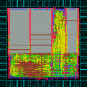
The "lookup table" is stored in the two SRAM microcells in the top left corner. The additional cell in the right is needed for the tree construction algorithm for building the table internally.
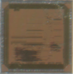
Produced Chip
I tried to scan the chip on my flatbed scanner, but of course without much luck ;). Remember, the chip has a side length of only 2.5 mm. Here is the result:
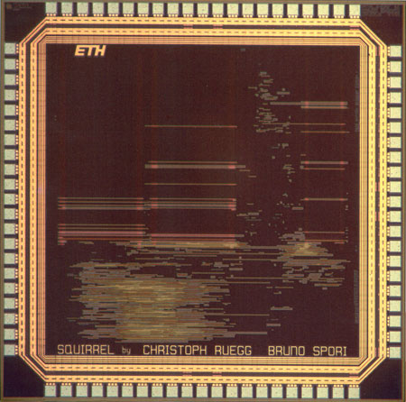
Luckily the microscope helps out. Here a better shot. Unfortunately you don't really see much of it, because the design center guys decided it would be better to fill the topmost metal 5 layer completely:
Nevertheless, it was a very interesting project. Let me know if you need a chip designer ;).
Testing
The testing went well: all tests succeeded and the timing behavior was as expected, even slightly better so we could overclock it to about 182 MHz at standard conditions (probably even more if we wouldn't test the async reset).